
Semiconductors are the materials, whose conductivity lies between metals and insulators. They are characterised by narrow energy gap (≈1eV) between the valence band and conduction band.
At room temperature all semiconductors behave like insulator.
On the basis of purity, semiconductors are of two types.
1. Intrinsic Semiconductors
2. Extrinsic Semiconductors
1. Intrinsic Semiconductors
An intrinsic semiconductors is also called an undopped semiconductor or I-type semiconductor. It is a pure semiconductor without any significant dopant species present.
Exp:- Pure Ge(Z=32) and Si(Z=14)
Ge = 2, 8, 18, 4 and Si = 2, 8, 4
Concept Of Electron(e⁻) and Hole Conduction
At temperature zero Kelvin the valence band is filled. The energy gap is 0.72 eV and the conduction band is totally empty.
Both Si and Ge have 4 electron in valenced shell and all four valence electron are involved in covalent bond formation. The nucleus has charge of + 4e and outer electron have total charge -4e.
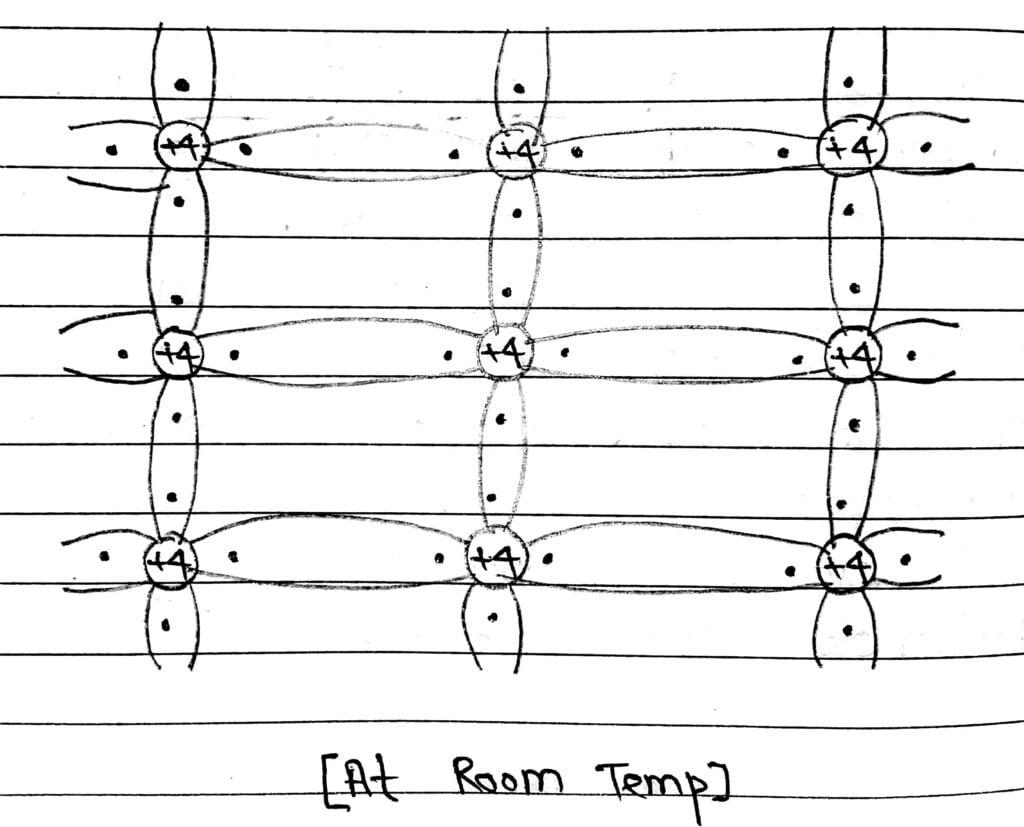
At room temperature there is no any free electron, because they involved in covalent bond.
# But when temperature increased, the covalent bond breaks and free electron are generated. The generated free electron moves to conduction band and available for Conduction under applied electric field.
# When electron removed from breaks of covalent bond, there is a vacancy created called hole. The holes has an effective positive charge equal and opposite to that of electron.
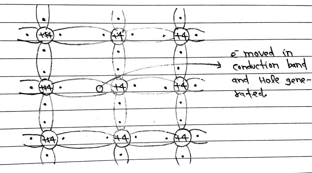
# Thus an intrinsic semiconductor, the number of holes and the number of free electron are equal.
# The hole created by electron are fill by neighbouring electron from covalent bond under electric field and a new vacancy would be created at its location.
# Now, this process gone continue. Since, there is a shifting of holes in the opposite direction of electron shift, So a new current Ih rise in semiconductor. This current is due to movement of valence band electrons.
# Thus total current I is the Sum of the electron current Ie and the whole current Ih.
Therefore I = Ie+Ih
Thermally excited electrons T > 0 Kelvin, partially occupy the conduction band.

2. Extrinsic Semiconductors
Those semiconductors in which some impurity atoms are embedded to improve the conductivity of pure semiconductor is known as extrinsic semiconductor
Extrinsic semiconductors are two types.
(I) n-type semiconductors
(II) p-type semiconductors
(I) n-type semiconductors
The semiconductors in which majority charge careers are electrons and minority charge careers are holes are called n-type semiconductors.
Formation Of n-types Semiconductors
When we dope pentavalent impurity atom Sb, Phosphorus(P), Arsenic(As) with pure silicon(Si) or Germanium(Ge) crystal, then 4 of its electron bond with the 4 silicon(Si) neighbours while fifth remains very weakly bound to its parent atom. The ionisation energy required to set this fifth electron free is very small (0.01 eV) for Germanium(Ge) and 0.05 eV for silicon(Si).
At room temperature these electron are almost free to move. Thus by adding pentavalent impurity, the number of free electrons in crystal increases
The pentavalent impurity donates one extra electron for conduction, Hence it is known as donor impurity.
Some free electron are also generated thermally due to breaking of few covalent bond and these number of free electron are equal to number of holes.
But as compared to free electrons, the number of holes are comparatively less, due to the presence of donated electrons, So the majority conduction of n-type semiconductor is due to electron, So electron are known as majority careers and holes are known as the minority careers.

(II) p-type Semiconductors
The semiconductors in which majority charge careers are holes and minority charge carriers are electrons are called p-type semiconductors.
Formation Of p-type Semiconductors
In p type semiconductors doping is done with trivalent impurity atoms. Trivalent atom are those which have three valence electrons in their valence shell.
Exp:- Indium(In), Boron(B), Aluminium (Al)
The impurity atom replaces a silicon(Si) or Germanium (Ge) atom in crystal.

Three valence electron of impurity atom (Al) from 3 covalent bonds and a valency(hole) is left out of site of impurity atom(Al).
When and electric field is applied, a neighbouring electron may jump to this hole and in this process a new hole is created. This happen across the crystal.
Some electrons and holes are also generated thermally due to breaking of covalent bonds. In this process the number of holes is equal to the number of electron.
Thus, the holes are majority charge careers and electrons are minority charge careers in p type semiconductors.
Note: For both p-type and n-type semiconductors-
Also Read: CBSE Class 12 Physics Chapter-14 (Semiconductor and Electronic Devices) All Topics