
A semiconductor diode is basically a P-N junction diode with metallic contact provided at the ends for the application of an external voltage. It is a two terminal device.
A P-N junction diode is represented by
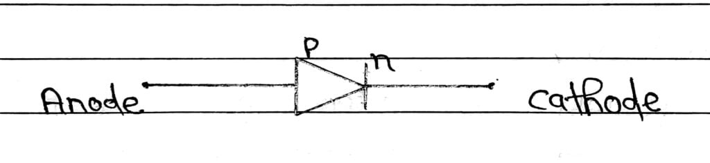
The direction of the arrow indicates the conventional direction of current.
Working of a P-N Junction Diode
The junction diode can be connected to an external battery into ways called forward biasing and reverse biasing of the junction.
Forward Biasing
A junction diode said to be forward biased when the positive terminal (higher potential) of the external battery is connected to the p-side and negative terminal (lower potential) to the n-side of the diode.
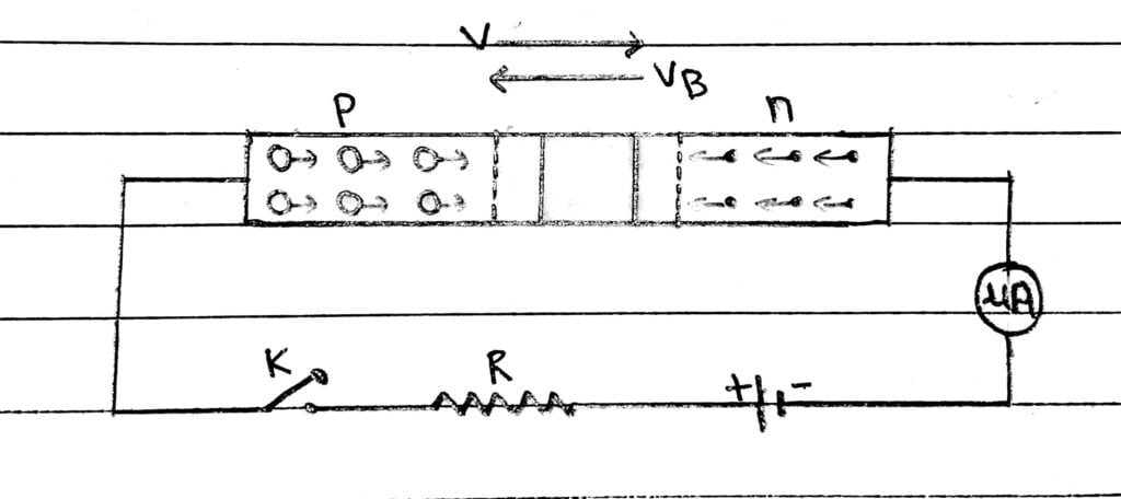
In forward biasing the applied voltage V opposes the barrier potential VB. As the result of this-
(I) The effective potential barrier decreases to (VB-V) and hence the Energy barrier across the junction decreases.
(II) The majority charge careers hols from p-side and electron from n-side begins to flow towards the junction.
(III) The diffusion of electrons and holes into the depletion layer decreases its width.
(IV) The effective resistance across the P-N junction decreases.
When V exceeds VB, the majority charge careers start flowing easily across the junction and setup a large current call Forward Current in the circuit. The current increases with the increase in voltage.
Reverse Biasing
If the positive terminal of the battery is connected to the n-side and the negative terminal of the p-side then the P-N junction is said to be reverse biased.
The applied voltage V and the barrier potential VB are in the same direction.
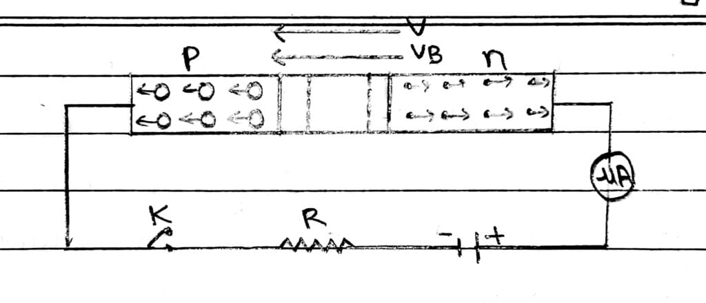
As the result of this-
(I) The battery potential increases (V + VB) and hence the Energy barrier across the junction increases.
(II) The majority charge careers move away from the junction, increasing the width of depletion layer.
(III) The resistance of the P-N junction becomes very large.
(IV) No current flow across the junction due to majority of charge careers.
As the minority charge careers are much less in the number then the majority charge careers, However a very small current due to minority charge careers flows across the junction. This current is called Reverse Current.
Also Read: CBSE Class 12 Physics Chapter-14 (Semiconductor and Electronic Devices) All Topics